Summary
NVIDIA and Cisco have announced plans for USFP, a pluggable optical-module form factor designed for 400Gb/s-per-lane signals and up to 12.8Tb/s of capacity. The companies say it could increase network bandwidth density while retaining a familiar pluggable deployment model.
NVIDIA and Cisco announced plans on October 12, 2026, for Ultra-Dense Small Form Factor Pluggable (USFP), a pluggable optical-module form factor designed for 400Gb/s-per-lane electrical signals. The companies say planned USFP transceivers will support up to 12.8Tb/s of overall capacity, giving AI data-centre networks a way to connect more computing systems within a similar front-panel footprint.
A pluggable transceiver links a device’s electrical interface to optical fibre, carrying data as light between network equipment. As AI systems grow, operators need more bandwidth between computing systems. NVIDIA and Cisco argue that adding network capacity through extra switch layers and optical links can also increase latency, power use and cost.
A higher-capacity module in an OSFP-sized footprint
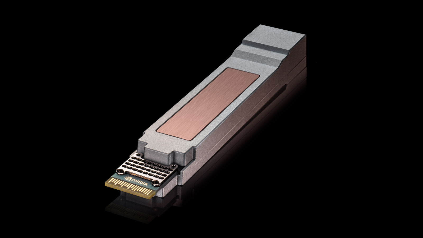
The first planned USFP transceivers will use 16 full-duplex lanes—channels that carry data in both directions—in a footprint comparable in size to an OSFP module. They are designed for use with switches and SuperNICs. NVIDIA and Cisco put USFP’s overall capacity at 12.8Tb/s and say the design could connect more 1.6Tb/s endpoints without adding network tiers. The connector is intended to support 32 full-duplex lanes and more in future configurations.
Compared with 200Gb/s-per-lane pluggable modules, the companies say USFP offers four times the bandwidth density and approximately 1.3 times the power efficiency. Their stated aim is to let AI infrastructure builders increase computing scale without expanding the network’s front-panel footprint, while reducing networking’s share of the facility’s power budget.
The physical interface is a central part of the proposal. USFP uses a two-dimensional array connector with a two-step insertion design: high-speed contacts engage after the module is inserted. NVIDIA and Cisco say this is intended to reduce contact wear, improve signal integrity and make insertion force more predictable. They also say the design supports power dissipation of up to 100 watts without a separate, dedicated embedded cooling circuit within the transceiver.
The release describes optical designs that simplify signal processing to reduce latency and power, with support for different optical technologies and connection distances. These capabilities are presented as design aims for the form factor, rather than results from a reported deployment test.
A shared hardware ecosystem is planned
NVIDIA and Cisco are working with TE Connectivity and Amphenol on USFP cages, connectors and modules. They say additional suppliers are expected to join. A shared form factor could give manufacturers a common basis for developing compatible hardware, while preserving the serviceability and deployment flexibility associated with pluggable transceivers.
The companies also plan to create an open industry specification through an upcoming community-led, multi-source project. USFP is therefore an announced design and ecosystem effort, with its first transceivers still described as planned. The specification project is intended to involve multiple suppliers rather than rely on a single company’s implementation.